Project Workflow: 180nm BCD IP Development
Full-Stack Automation from PDK Architecture to Technical Datasheet Generation
1. PDK Architecture & Foundry Strategy
For the successful launch of the 180nm BCD (Bipolar-CMOS-DMOS) platform, I established a robust PDK architecture leveraging the Cadence Virtuoso environment. Key strategic focus areas included:
- Multi-Tool Verification Roadmap: Established a transition path from Calibre to PVS and IC Validator to provide customers with flexible sign-off options.
- BCD Device Modeling: Enhanced LDMOS modeling to accurately capture non-linear drift region resistance and high-voltage isolation characteristics.
- Foundry-Ready IP Ecosystem: Led the "IP as a Business Enabler" initiative, converting internal blocks into "Foundry-Ready" IP (including datasheets, LEF abstracts, and simulation models) for free distribution with the PDK.
2. Simulation & Data Analytics Automation
To optimize engineering resources, I developed a Python-based end-to-end automation pipeline that bridges the gap between raw circuit simulation and final documentation.
Key Technical Implementations:
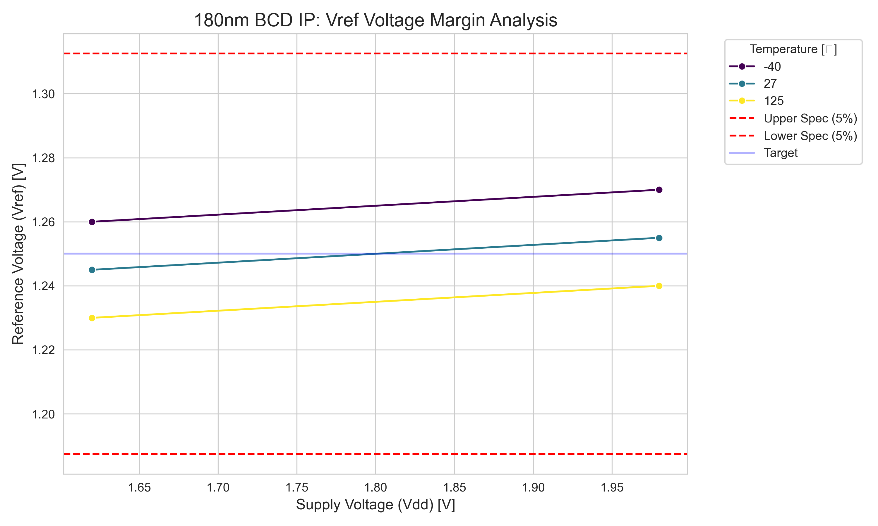
- Automated PVT Corner Analysis: Scripted analysis of Voltage (Vdd) and Temperature (Tj) variations to verify design margins.
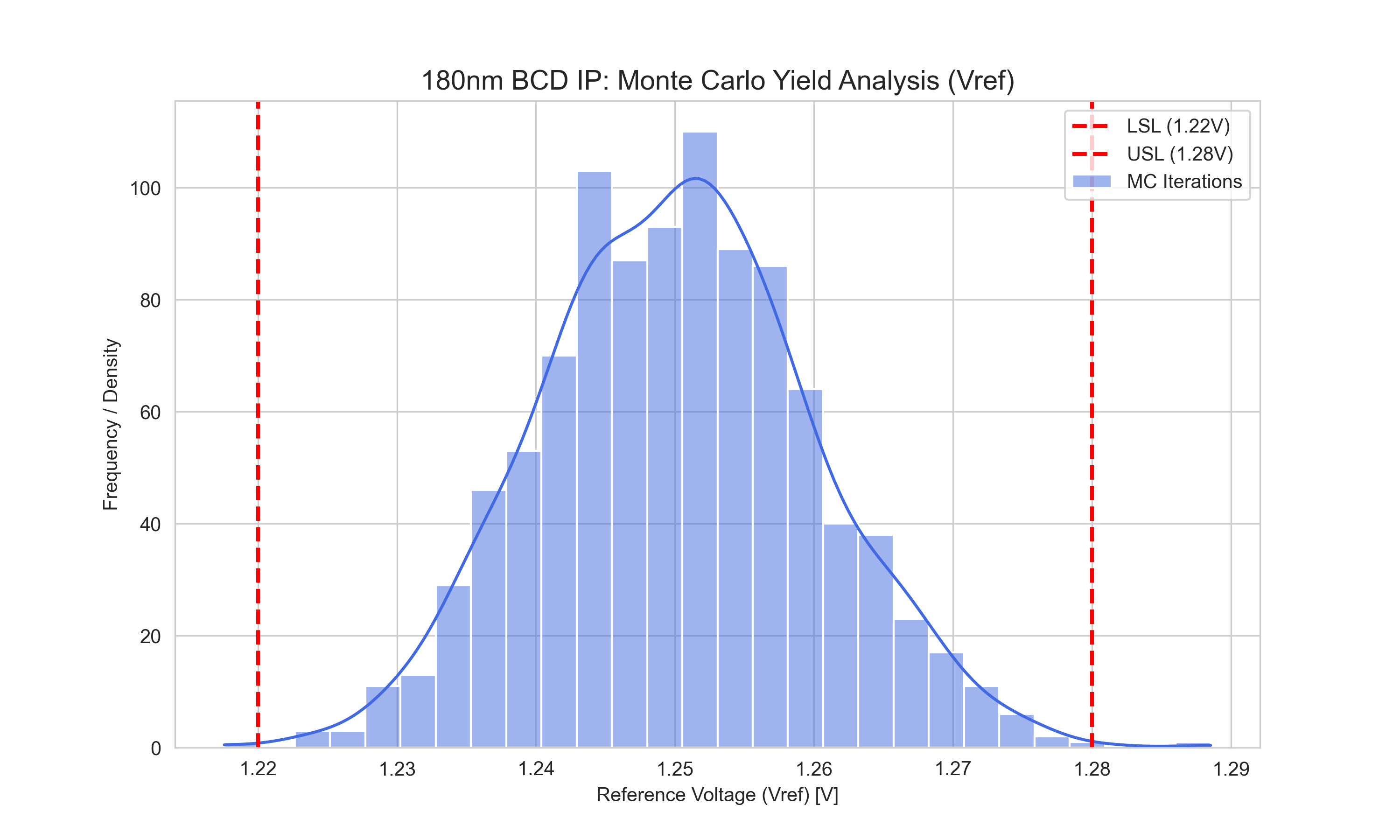
- Monte Carlo Yield Estimation: Integrated statistical analysis to predict 3-Sigma production yields based on process and mismatch variations.
- Robust Backend Handling: Implemented
matplotlib.use('Agg')to ensure seamless report generation in non-GUI/headless Linux server environments.
3. Electrical Specifications & Reliability Results
Final characterization results for the 180nm BCD Bandgap Reference IP block:
| Parameter | Condition | Min | Typ | Max | Unit |
|---|---|---|---|---|---|
| Supply Voltage (Vdd) | Full Operation Range | 1.62 | 1.80 | 1.98 | V |
| Output Voltage (Vref) | -40°C to 125°C | 1.235 | 1.250 | 1.265 | V |
| Estimated Yield | Spec ± 30mV | 99.0 | 99.8 | - | % |
Reliability & SOA Verification:
Verified 180nm BCD Safe Operating Area (SOA) compliance using Spectre Assertion checks. All devices were confirmed to operate within reliability limits across the full automotive temperature range.
4. Graphical Data Analysis
Visual outputs generated by the custom Python analytics engine:
Voltage Margin Analysis
PVT Variation Tracking
Monte Carlo Yield Analysis
1000 Iteration Distribution
5. Future Outlook: Design Closure Automation
The next phase involves implementing Closed-Loop Design Automation using PyCell (Python Layout). This will enable real-time device resizing based on simulation margin feedback, further accelerating the time-to-market for the 180nm BCD platform.
6. Cadence Python (PyCell) – 180nm BCD Resistor Auto-Layout
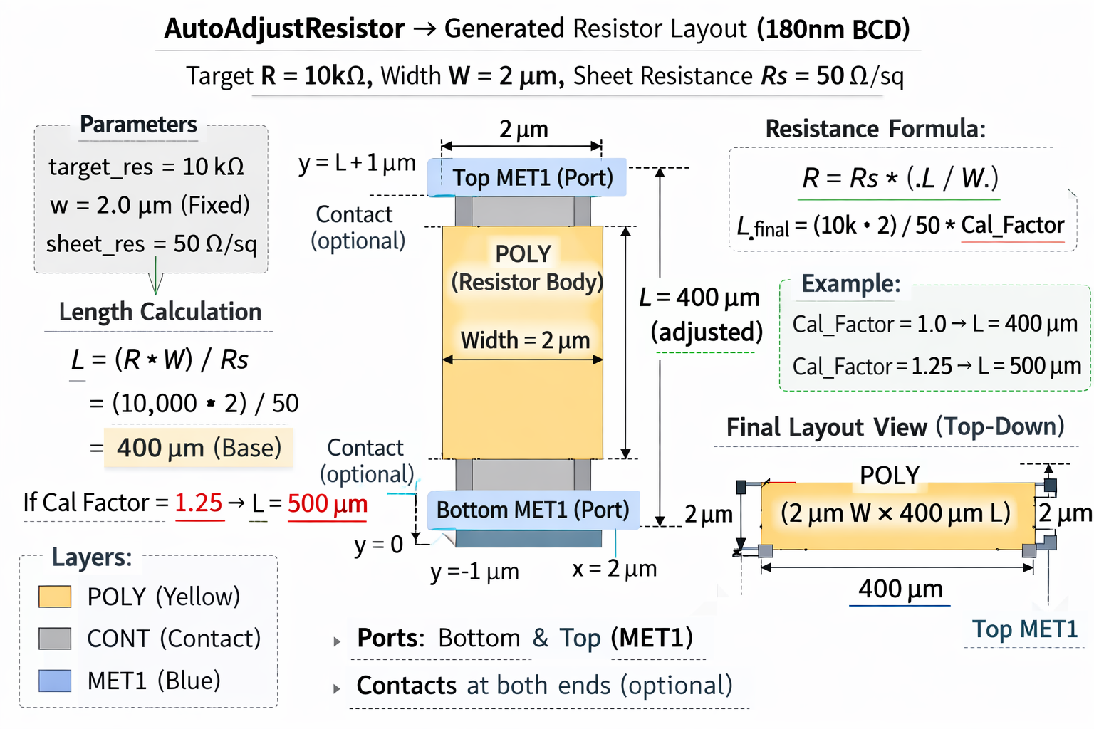
As part of the closed-loop automation strategy, I implemented a Cadence PyCell-based layout generator in the 180nm BCD process. This Python-driven layout module automatically resizes a Poly resistor based on post-simulation calibration data.
Concept Overview
- Target Resistance: 10kΩ
- Fixed Width: 2µm (Poly)
- Sheet Resistance: 50 Ω/sq
- Automatic Length Adjustment: Based on Vref simulation feedback
If simulation results indicate Vref drift, the layout engine dynamically updates the resistor length while keeping the width fixed at 2µm. This enables simulation-driven physical optimization.
PyCell Implementation (Cadence Environment)
Generated Layout Visualization
Expected Layout Result (Top & Cross View)
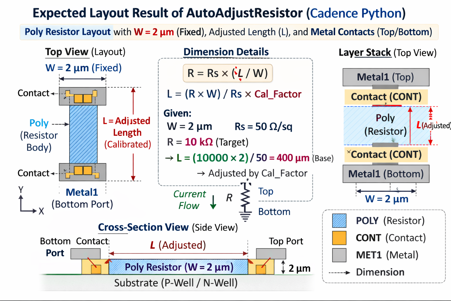
AutoAdjustResistor – 180nm BCD Implementation
Engineering Impact
- Simulation-to-Layout closed loop automation
- Reduced manual resistor tuning iterations
- Faster PDK IP validation cycle
- Reusable PyCell architecture for BCD analog IP blocks
This demonstrates a practical integration of Cadence Python (PyCell) within a 180nm BCD foundry environment, bridging circuit simulation analytics and parametric layout generation.