Advanced-Node Layout Architecture
Below the 14nm node, layout design is no longer about drawing shapes.
It is about explicitly constraining degrees of
freedom
to ensure manufacturability, yield
stability,
and predictable OPC convergence.
At advanced technology nodes, a large class of geometries can be fully DRC-clean yet fundamentally non-manufacturable. This disconnect exposes the limits of traditional rule-based layout validation.
As a result, the role of layout automation and PCells must fundamentally change.
PCells must move beyond parameterized geometry generation
and instead encode manufacturing intent directly into the layout
architecture.
Architectural Perspective
A robust advanced-node layout architecture follows a strictly ordered pipeline:
User Parameters
↓
Topology Definition
↓
Technology Rules (PDK)
↓
DFM / OPC Guards
↓
Layout Geometry
Each stage deliberately removes freedom rather than adding it.
Invalid structures are not fixed after the fact —
they are architecturally impossible to generate.
Good layout architecture removes freedom, not adds it.
Refactored FinFET (12nm) PCell Architecture
Whiteboard Overview
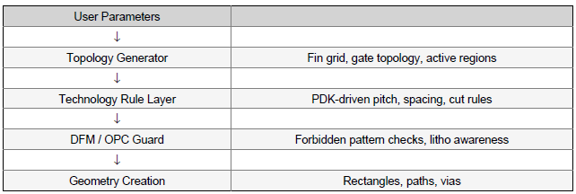
This diagram illustrates a topology-driven PCell architecture designed for advanced FinFET nodes (12nm and below).
The central principle is simple but critical:
Topology is defined first.
Technology constraints are applied second.
Geometry is created last.
This ordering ensures that all generated layout is inherently manufacturable.
Architecture Flow
User Parameters
High-level design intent and device configuration
↓
Topology Generator
- Fin grid definition
- Gate topology
- Active region structure
↓
Technology Rule Layer
- PDK-driven pitch enforcement
- Spacing constraints
- Cut and coloring rules
↓
DFM / OPC Guard Layer
- Forbidden pattern prevention
- Lithography-aware checks
- Yield-driven constraints
↓
Geometry Creation
- Rectangles
- Paths
- Vias
Geometry is treated as a final artifact,
not a design space.
Key Message
At advanced nodes, effective PCells do not generate shapes.
They encode manufacturing intent,
enforce topological correctness,
and prevent non-manufacturable structures by construction.