Comparison Diagram
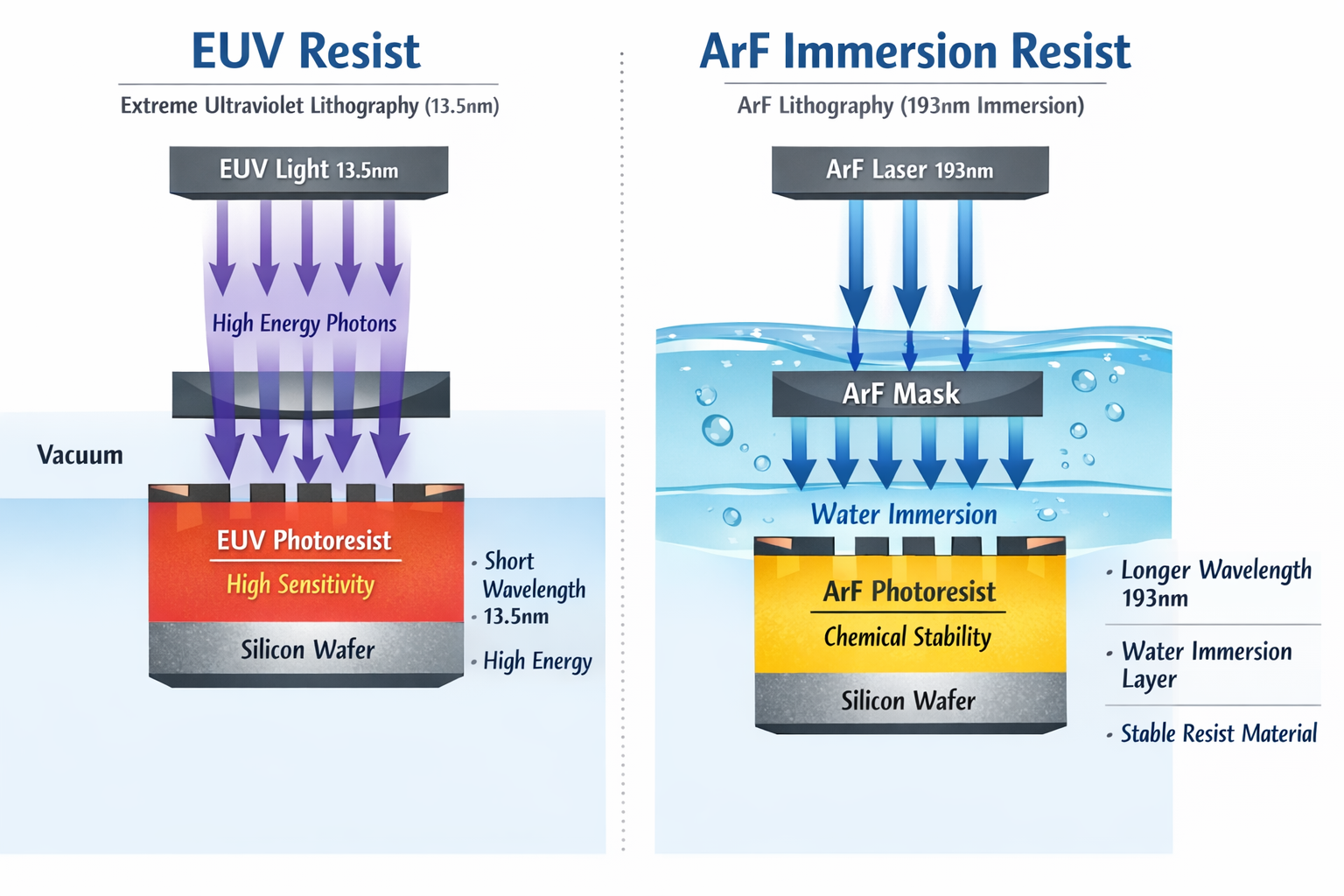
In semiconductor manufacturing, lithography is used to transfer circuit patterns onto silicon wafers. The wavelength of light used in lithography determines the resolution of patterns that can be achieved. EUV and ArF immersion lithography are two advanced technologies used for different process nodes.
When a material or process is compatible with both EUV and ArF immersion lithography, it means the resist, mask, or equipment can function in both lithography processes while maintaining performance and pattern quality. This provides process flexibility and reduces development costs.
↩ Go to OPC / RET Technical Notes Index
↩ Go to Home – Tech Notes Park